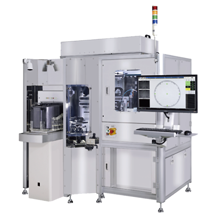
WP-MM3200
SHUZ TUNG(WisePioneer) MACHINERY INDUSTRIAL CO., LTD.
Applications:
Semiconductor wafer packaging, testing and related industries
Semiconductor mid-end process equipment
. Front-end process: ADI, AEI, ASI….etc.
. Advanced Packaging: Wafer Thinning, Bumping process
. For wafers: 8"" & 12""
Main functions:
Fully automatic wafer inspection (macro & micro)
According to customer needs, it can perform macroscopic inspection of wafers such as: wafer corner chipping, cracks, abnormal wafer engraving, residual tin on the edge, etc. Supplemented by AI for defect classification; at the same time, it can perform microscopic inspection of wafers such as critical dimensions, offset, etc.
It can replace manual operations, improve the speed and accuracy of wafer inspection, reduce false detection rate, and automatically report, store and analyze data. Meets the needs of smart production.
· Fully automated wafer macroscopic inspection/micro inspection measurement
· AOI+AI software defect detection and classification
Product Features:
◆Automatic macro and micro inspection for pattern and unpattern (bare wafer) wafer
◆AOI defect detection and AI-assisted classification
◆Defect Inspection
- Micro Objective Lens: 5X, 10X, 20X, 50X, 100X or optional
- Macro Resolution: £ 20 µm
- Inspection Items: Wafer Top, Bottom, Side
◆Critical Dimension Measurement
- 2D Accuracy ≦ 1 µm
- GR&R ≦ 5%
◆Automatic Focusing: Optical Confocal and Imaging Focusing
◆Software Function: Defect Inspection, CD Measurement, SECS/GEM